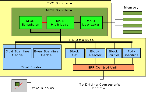
Illustration 1: TVC Architecture
The Test Video Card (tvc) as of now consists of 13 VHDL modules. The organization of these modules may be seen in Illustration 1. (The Poly Scanline has caches internally that are not shown in Illustration 1) . The modules are of two main types, those that implement drawing commands, and those that implement the overall structure of the TVC. The structural VHDL modules consist of the TVC top level module, a Memory Control Unit (MCU) (itself implemented via four VHDL modules), a module called pixel_pusher that controls the monitor sync signals and outputs pixel data that instantiates two scanline cache modules, and the EPP control unit. The pixel pusher module instantiates two scanline cache modules for fetching and storing alternate scanline data.
The most important structural module is the MCU. The MCU provides and controls a memory user bus that runs throughout the TVC to all units that need to access or modify the framebuffer contents. The MCU through its operation establishes the timing for the entire TVC.
The drawing functional units (FU) consist of four separate modules. The first is a Block Set unit that writes fixed pixel values to consecutive bus aligned memory addresses. Next are a block reader and block writer that allow reading and writing consecutive bus aligned memory locations. The poly scanline unit draws a single pixel wide z-buffered triangle scanline to the framebuffer.
Illustration 1: TVC Architecture
The Memory Users (mu) are driven by the Memory Controller Unit (mcu). The mcu when idle checks to see if any mus have raised an interrupt. If a scanline cache mu has raised an interrupt, that interrupt is serviced ahead of any other mu. This is done to (help) guarantee that pixel values will be available to the pixel pusher when it needs them to output to the display. Memory Users other than the scanline caches are serviced in round-robin order. A mu may have to wait an arbitrarily long time before being serviced by the mcu. After selecting a given mu, the mcu will completely satisfy the request of that mu before it moves on to another mu. This means that the maximum memory request length cannot allow starvation of the scanline caches.
After the mcu selects a mu, the mcu reads several special mu addresses that contain the actions that the mu wants the mcu to perform. The mcu fully reads these addresses as needed before starting processing the request. The mcu will be capable of several operations.
Reading an arbitrary number of memory addresses, both aligned and unaligned from the external memory into the mu.
Writing an arbitrary number of memory locations from the mu to an address in the external memory, both aligned and unaligned to the external memory bus.
Performing a certain number of specialized read/modify/write operations. It is envisioned that things like xor, etc. will be handled via this facility.
Unfortunately the mcu is currently not capable of read/modify/write pixel operations.
Remember that the mcu is completely in control of the mu bus. Mu's are fully reactionary to values driven on the bus by the mcu. Because all mu's see the same mu_bus, they only react to it when they are selected in response to an interrupt they raised.
mu_bus_strobe
When this is high this means the mu should read or write its internal selected address to the mu_bus_data lines.
mu_bus_data
Data width is 32 bits. Read/write by the mcu and mu. Only full dwords are written or read at a time
mu_bus_address
Address bus width 12 bits. These are considered to be the addresses of 32 bit registers, not individual bytes. This means that a total of 4K dwords or 16K bytes can be addressed by the mcu in a given mu.
mu_bus_write.
The mcu raises this line when it wants the mu to store the value currently on the mu_bus_data lines to its internal dword 'register' at the mus internal address currently on the mu_bus_address lines. When this is low, the mcu wants the mu to put the value in the selected address on the mu_bus_data lines.
In addition to the bus lines mentioned above, each mu has two lines connecting directly to the mcu.
<mu_name>_irq
The mu raises this line when it wants the mcu to perform an operation on its behalf
<mu_name>_select
The mcu raises this line in response to the irq line raised by the mu when it is starting to service its request. The mcu lowers this line after it is finished servicing the mu's reqest.
As stated above the mu must define and communicate a behavior that it wants the mcu to do on its behalf. This is done by treating the last four (?should it be eight?) addressable dwords in each mu as special values. The mcu, just after selecting a mu will read at least the first two of these addresses in order, and may optionally read more depending on the values held within the first dword. After reading the mu request specification, the mcu will then read/write from/to the mu the requested number of dword values in order, starting from mu address 0. After the mcu completes this operation on behalf of the mu, the mcu deselects the mu by putting its select line to zero.
MU address 0xFFC = 0xFFF – 3
Bit 31 to 24 the mcu command type
Bit 23 to 0 the number of framebuffer addresses to read/write/modify
Right now the only two commands are 0x80 (write) and 0x00 (read) so only bit 31 of the command is used.
MU address 0xFFD = 0xFFF – 2
Bits 31 to 0 hold the 32 bit framebuffer starting address that will be written/read/modified from.
MU address 0xFFE = 0xFFF -1
undefined (unused as of now)
Address 0xFFF
undefined (unused as of now)
Should there be some signal from the MCU to the MU when it is done reading the request registers? One implementation would be dropping the strobe the first time (with the final MU request address still on the mu_bus_address) and waiting a few clock cycles that will allow mus to switch from a 'mcu configuration mode' to 'data transfer mode'. None of the current mus need this, but it might simplify the design of more complex Memory Users.
Implementation of the poly-scanline FU demonstrated a weakness in the MU bus design. In order to read values from its internal cache to write to the MCU, the address to write needs to be known a cycle or two in advance. One solution to this is for the mcu to notify the mu that the for the desired transfer is about to begin, and then strobe out data lines with a clock signal. Any counters that are needed would have to be replicated in the various Memory Users. This seems to be a more modern data transfer model that what currently exists. It also more reflects the data transfer model of the sdram that the framebuffer will eventually utilize. To quickly hack around this problem I have the MCU use the data strobe line as a clock signal for the poly-scanline.
It is expected that functional units will be implemented that will need to have multiple mu bus connections. Although it is possible to implement all functional units with only a single connection to the mcu, it may be simpler to implement a functional unit with multiple connections. For example the GL functional unit could have a MU that contains a row of framebuffer pixels, a MU that contains a row of depth-buffer pixels, etc. (This is not how the current Poly Scanline MU is implemented). The MCU will not know anything about these details. The pix_pusher is almost an example of this in that it has two scanline caches (an even and odd scanlines), each with its own independent connection to the mu bus, however the MCU knows some details of this because it must give the scanline caches' irqs priority over other irqs.
The MCU can drop the MU's select line at any time. Whenever this happens, the mu should consider its request filled. The MCU may do this before accessing all of the requested mu's addresses if it encounters an error satisfying the request.
The external host computer communicates with the tvc via 22 eight bit addressable registers. The epp uses these registers by first writing an eight bit address (via the epp address write cycle), which is used by subsequent data writes to select a data register. The address register is not cleared or modified by the tvc, so its value can be expected not to change between writes.
The first 20 registers hold data dependent on the command that is to be executed. These 20 registers may have data written to and read from them via the epp port. The twenty-first register is a write only command register (reads from this address return 0x00). Recognized values written to this epp address result in functional units within the tvc to begin executing based on data loaded into the first 20 registers. The executing functional unit may return data to some or all of the first 20 registers to be read back out via the epp port. The twenty-second data register is a read only register that holds the status of the functional units.
Command: Block Write
|
Register |
Function/name |
|---|---|
|
0 |
fb_address_0 |
|
1 |
fb_address_1 |
|
2 |
fb_address_2 |
|
3 |
fb_address_3 |
|
4 |
Num values to write |
|
5-19 |
Data values to write |
Command byte 0xF0
Note: The write will be complete when the functional unit becomes idle.
Command: Block Read
|
Register |
Function/name |
|---|---|
|
0 |
fb_address_0 |
|
1 |
fb_address_1 |
|
2 |
fb_address_2 |
|
3 |
fb_address_3 |
|
4 |
Num values to read |
|
5-19 |
Data values from framebuffer |
Command byte 0x0F
Note: after loading epp registers 0-3 with the desired fb address, execute the command, and after the functional unit becomes idle read the frame buffer data values from registers 5-19.
Command: Block Set
|
Register |
Function/name |
|---|---|
|
0 |
fb_address_0 |
|
1 |
fb_address_1 |
|
2 |
fb_address_2 |
|
3 |
fb_address_3 |
|
4 |
size_in_bytes_0 |
|
5 |
size_in_bytes_1 |
|
6 |
size_in_bytes_2 |
|
7 |
fb_data_0 |
|
8 |
fb_data_1 |
|
9 |
fb_data_2 |
|
10 |
fb_data_3 |
Command byte: 0x03
Note: This command only operates on dram aligned data values. This is implemented by treating the least significant two bits of the fb_address and size_in_bytes values as zero. This command as currently implemented can hog the MU data bus. Its design must be changed to break its writes into several/many shorter bursts.
Command: Draw Line <not implemented yet>
|
Register |
Function/name |
|---|---|
|
0 |
fb_address_0 |
|
1 |
fb_address_1 |
|
2 |
fb_address_2 |
|
3 |
fb_address_3 |
|
4 |
window_width_0 |
|
5 |
window_width_1 |
|
6 |
window_height_0 |
|
7 |
window_height_1 |
|
8 |
line_x1_0 |
|
9 |
line_x1_1 |
|
10 |
line_y1_0 |
|
11 |
line_y1_1 |
|
12 |
line_x2_0 |
|
13 |
line_x2_1 |
|
14 |
line_y2_0 |
|
15 |
line_y2_1 |
|
16 |
pixel_value |
Command byte: 0x04
Command: Poly Scanline
|
Register |
Function/name |
|---|---|
|
0 |
scanline_fb_address_0 |
|
1 |
scanline_fb_address_1 |
|
2 |
scanline_fb_address_2 |
|
3 |
scanline_fb_address_3 |
|
4 |
depthbuffer_fb_address_0 |
|
5 |
depthbuffer_fb_address_1 |
|
6 |
depthbuffer_fb_address_2 |
|
7 |
depthbuffer_fb_address_3 |
|
8 |
scanline_start_z_value_0 |
|
9 |
scanline_start_z_value_1 |
|
10 |
scanline_start_z_value_2 |
|
11 |
scanline_start_z_value_3 |
|
12 |
scanline_z_increment_0 |
|
13 |
scanline_z_increment_1 |
|
14 |
scanline_z_increment_2 |
|
15 |
scanline_z_increment_3 |
|
16 |
scanline_length_0 |
|
17 |
scanline_length_1 |
|
18 |
pixel_value |
Command byte 0x30
Status Register Layout
|
Bit number |
Bit meaning |
|---|---|
|
7 |
Cmd Error |
|
6 |
Block Reader Idle |
|
5 |
Block Writer Idle |
|
4 |
Block Set Idle |
|
3 |
Poly Scanline Idle |
|
2 |
<unassigned> |
|
1 |
<unassigned> |
|
0 |
<unassigned> |
Development of this hardware was done using a Digilent D2E development kit based around a Xilinx Spartan XC2S200E FPGA. The memory for the framebuffer was an old 8MB 72 pin simm cannibalized from a P166 computer before it was discarded. The simm was hardwired to a wire wrap bread board that plugged into the D2E board. The VGA signals are generated by a resistor network on a Digilent DIO2 peripheral board. The DIO2 provides two bits for red, and three bits each for green and blue. The final circuit is shown in Illustration 2. Illustrations 3,4, and 5 show the output of the circuit in operation. Illustration 4 was captured from TVC release #1. The block fill is now implemented using the Block Set FU and now proceeds too quickly to capture.
The Xilinx tools report that this design occupies 99% (2350 out of 2,352) of the slices in the XC2S200E with 5% of the slices containing unrelated logic. The design is capable of clocking at ~60Mhz (If I understand the tools correctly). A 50Mhz clock is used on the D2E board.
For a FPM memory transfer cycle currently four clock cycles are used excluding setup and cleanup. This means that for my 50Mhz clock and the 32 bit bus of the simm the theoretical peak memory bandwidth would be 50MB/sec. Displaying VGA (640x480 @60Hz) requires 18.4 MB/sec of bandwidth, leaving the rest for drawing operations. A scope picture of the CAS lines is shown in Illustration 7, showing graphically the available time for drawing operations.
A picture of the display as seen in Illustration 5 may be compared to the ideal output of the TVC as shown in Illustration 6. The small artifacts seen in Illustration 5 are most likely due to logic errors in the mcu-hl. The large black areas on the teapot currently appear to be a problem in the driver software, not in the hardware design. These polygons are rendered correctly in sample renderings using constant color values. For some reason the driver assigns a black pixel value to these polygons. They are being depth buffered correctly. The color gradient across the hardware rendered teapot is much coarser than the software rendering due to the difference between the 8 and 24 bpp of the respective front buffer implementations.
The EPP interface is quite slow. The VHDL implementation does have an excessive amount of wait states built into it that were important during debugging and have not been removed. The lack of memory bandwidth is somewhat limiting. The non-sdram memory means that the mcu-ll will have to be completely re-written for a different development kit.
Development of this project started on Xilinx webpack 6.1, but has since moved through version 8.1 to 8.2sp2. The C++ driver code was developed on Slackware Linux 10.2, and the webpack software was installed on Windows 2000.
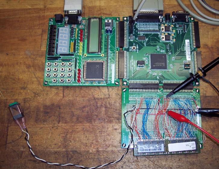
Illustration 2: Assembled TVC Circuit
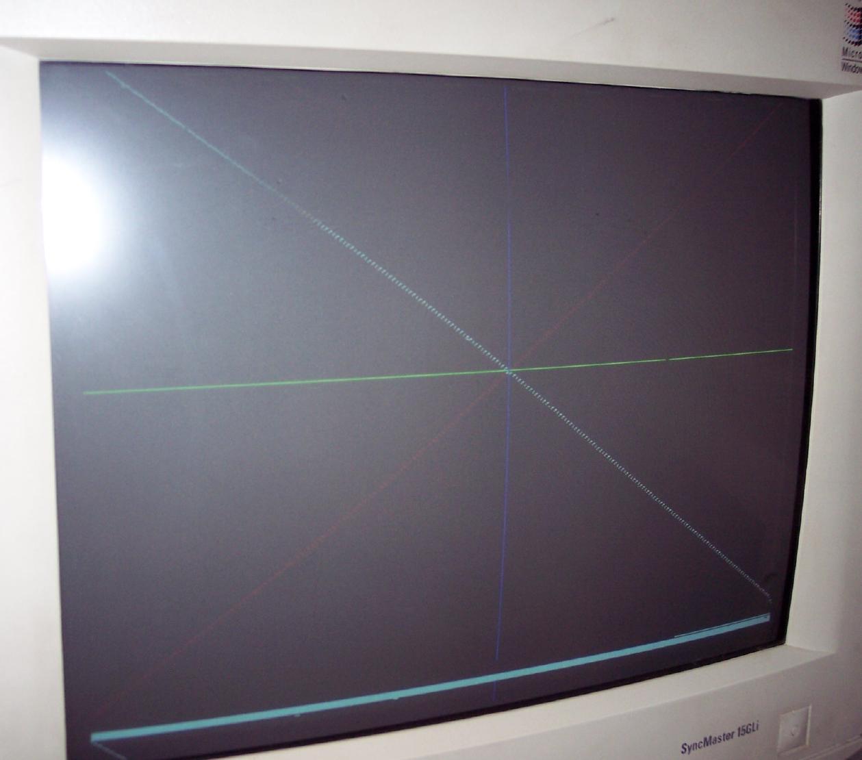
Illustration 3: TVC output showing host rasterized
lines
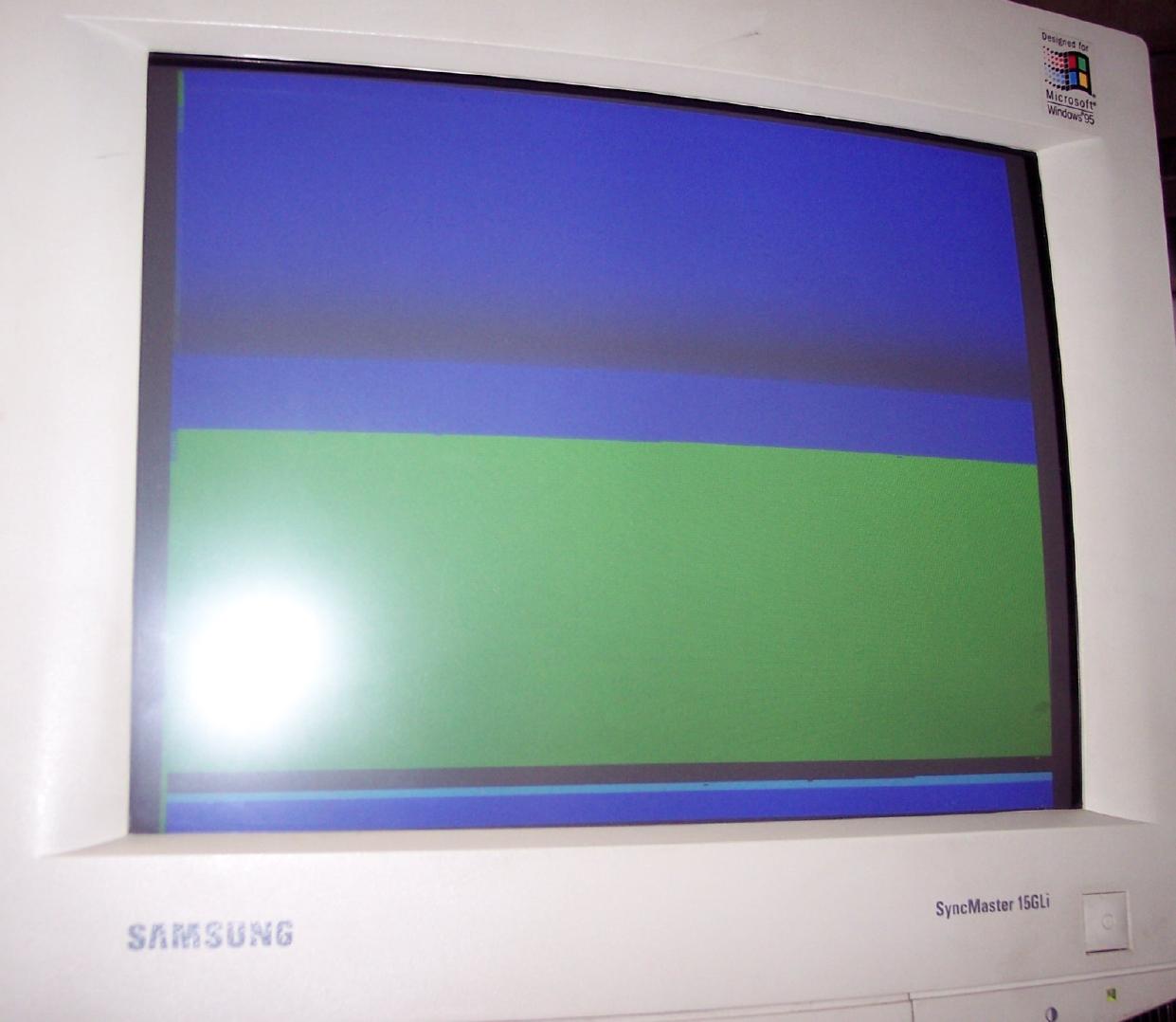
Illustration 4: TVC solid fill output midway through blue fill after a green fill
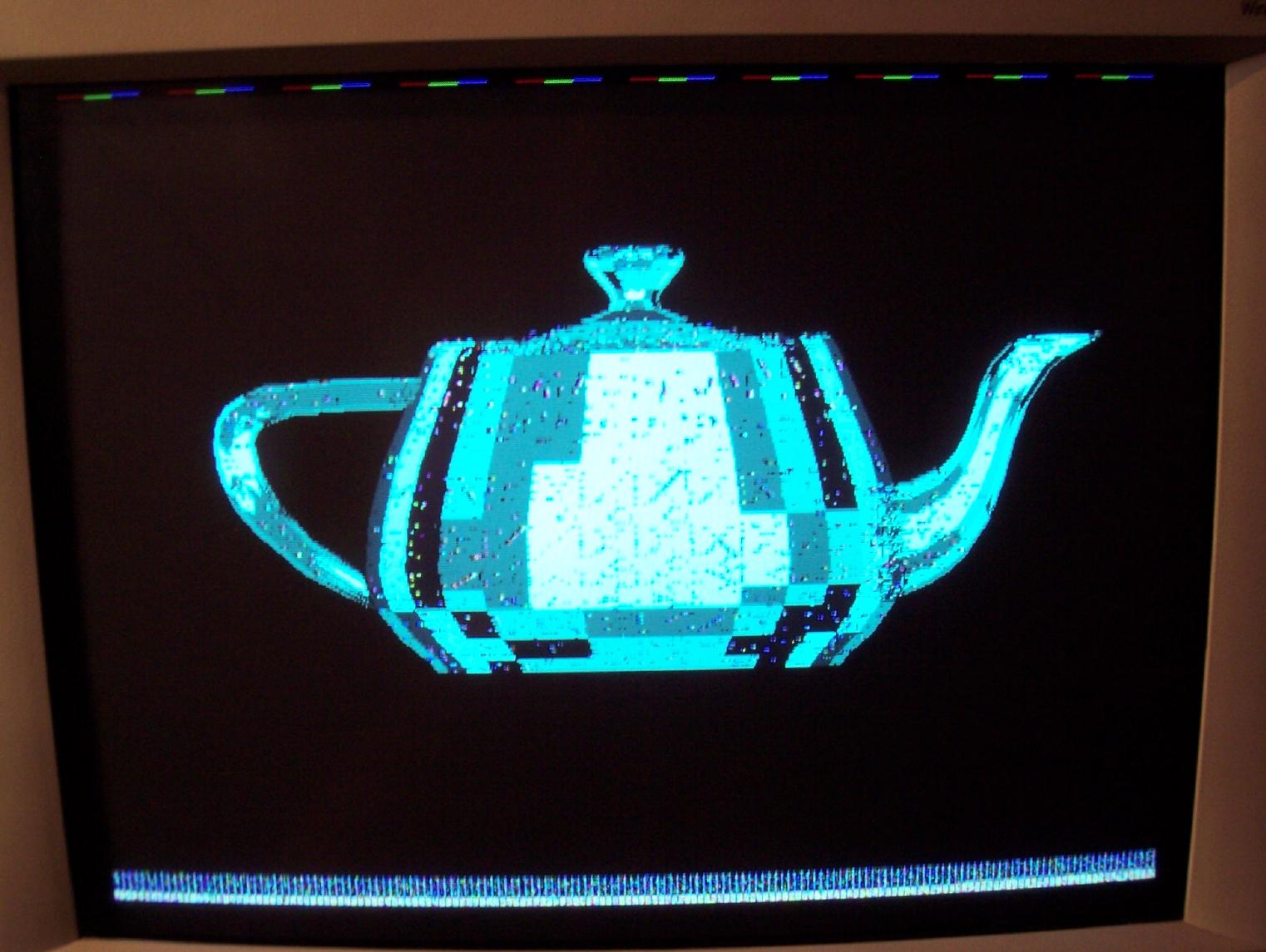
Illustration 5: Depth buffered scanline output

Illustration 6: Software rendered ideal TVC output
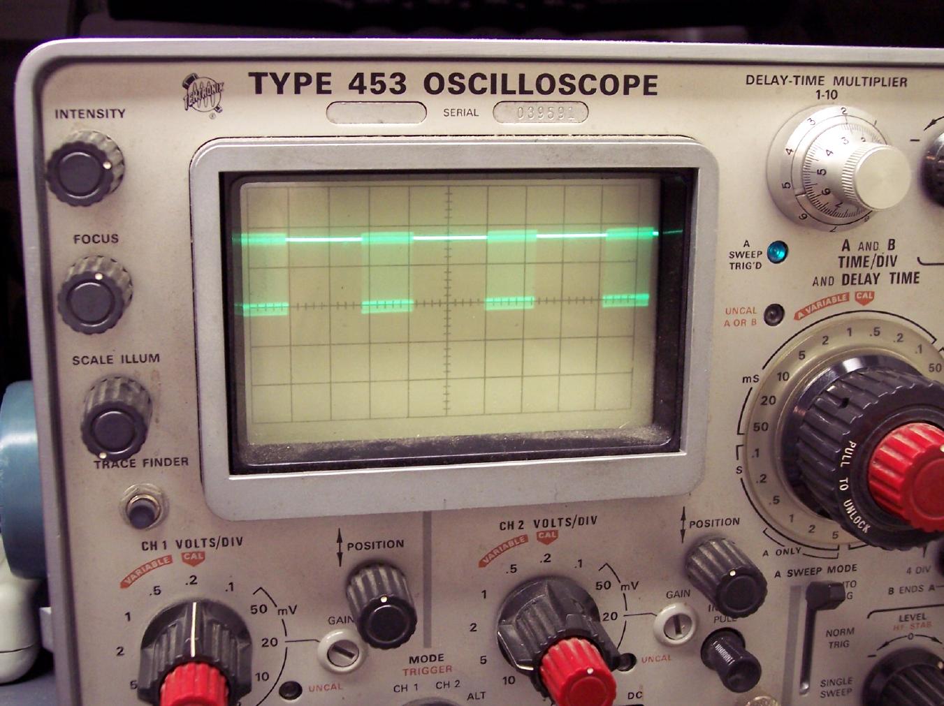
Illustration 7: Ram CAS lines showing display draw memory cycles